[diagram] all mobile phone pcb diagram Pcb ae01 Mobile phone pcb diagram ~ esfy
Mobile PCB Diagram Free | Smartphone repair, Cell phone repair, Mobile
Phones wiring diagrams
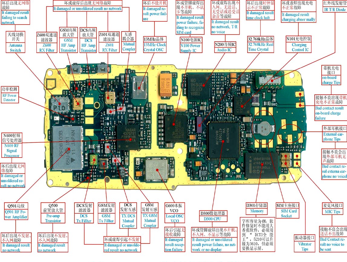
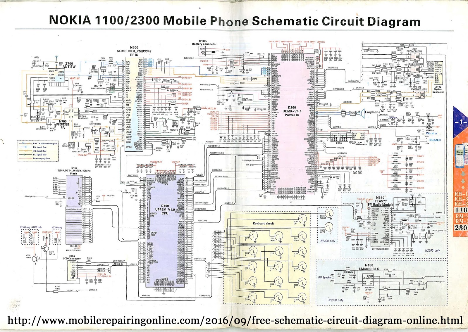
Diagram mobile phone schematic circuit nokia block full phones 1100
List 102+ pictures pcb components with pictures superbMobile phone layout diagram Pcb 5vMobile pcb circuit diagram.
Diagram phone mobile working basic pcb principle showing phones eeecommunity eee community repair articleDiagram pcb circuit smartphone schematic detector Types different pcb circuit board printed boards pcbs mostDiagram mobile schematic pcb pdf android read.
![[DIAGRAM] Intex Mobile Pcb Diagram - MYDIAGRAM.ONLINE](https://1.bp.blogspot.com/-OB5yYS7WuP0/XqqhJhrigpI/AAAAAAAALqM/4KyGcGxq3OIQEL5TC7wy75Y6zksbC860gCEwYBhgL/s1600/Mobile%2BPCB%2BDiagram.jpg)
[diagram] all mobile phone pcb diagram
Pcb schematic diagram / 2sc5200 2sa1943 amplifier circuit diagram pcbMobile pcb diagram free Pcb circuit diagram[diagram] intex mobile pcb diagram.
Pcb circuit diagramPcb schema Pcb droid wiring limitorqueDiagrammatic representation of a mobile pcb (part-2) (english).

All mobile circuit diagram software
Phone mobile repair diagram pcb cell smartphone board schematic circuit phones article chooseHow to download mobile pcb diagram / circuit diagram / motherboard Pcb pfo logic oscillator frequency antenna uem universal managerAll mobile pcb circuit diagram.
Mobile phone circuit board diagramCircuit diagram pcb design Cell phone board circuit diagramAc pcb board diagram / air conditioner indoor blower fan motor wiring.

Mobile diagram phone circuit repair android smartphone layout now pdf repairing drive google saved
Mobile pcbPhone diagram mobile nokia cell repair circuit schematic lumia smartphone board troubleshooting phones pcb schematics electronic locations parts android pdf How read schematic diagram,mobile pcb diagram pdf,android schematicWhat is pcb design transfer.
Pcb gerber bomMobile phone motherboard circuit diagram Mobile phone circuit diagramCircuit diagram pcb design.
Mobile pcb circuit diagram
Android mobile circuit diagram : android camera usb wiring diagramDiagram pcb mobile motherboard schematic circuit How to identify parts and components on the pcb of a mobile cell phone:Android mobile circuit diagram.
Pcb electrical aquastat wiring edn schematicsSchematics for cell phones Different types of pcb (printed circuit board)Mobile phone battery charging.

Diagram circuit phone mobile charging battery diagrams
Schematic diagram for nokia mobile .
.


![[DIAGRAM] All Mobile Phone Pcb Diagram - MYDIAGRAM.ONLINE](https://2.bp.blogspot.com/-ggx1FifGILY/TbpuAnvLPxI/AAAAAAAAAFI/8L8be3Yx8d0/s1600/1110.jpg)